
You're now following
Error following user.
This user does not allow users to follow them.
You are already following this user.
Your membership plan only allows 0 follows. Upgrade here.
Successfully unfollowed
Error unfollowing user.
You have successfully recommended
Error recommending user.
Something went wrong. Please refresh the page and try again.
Email successfully verified.

ahmedabad, india
It's currently 9:03 AM here
Joined April 21, 2016
1 Recommendation
Maulik P.
@maulik1717
3.6
3.6
100%
100%
ahmedabad, india
100%
Jobs Completed
11%
On Budget
11%
On Time
50%
Repeat Hire Rate
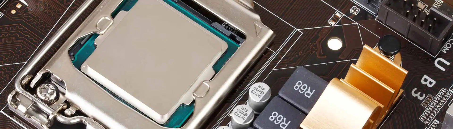
Pcb layout in allegro and altium. DFM in genesis
Contact Maulik P. about your job
Log in to discuss any details over chat.
Portfolio
Portfolio
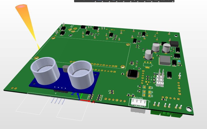

Pcb Layout of Automatic hand sanitizer.

Pcb Layout of Automatic hand sanitizer.
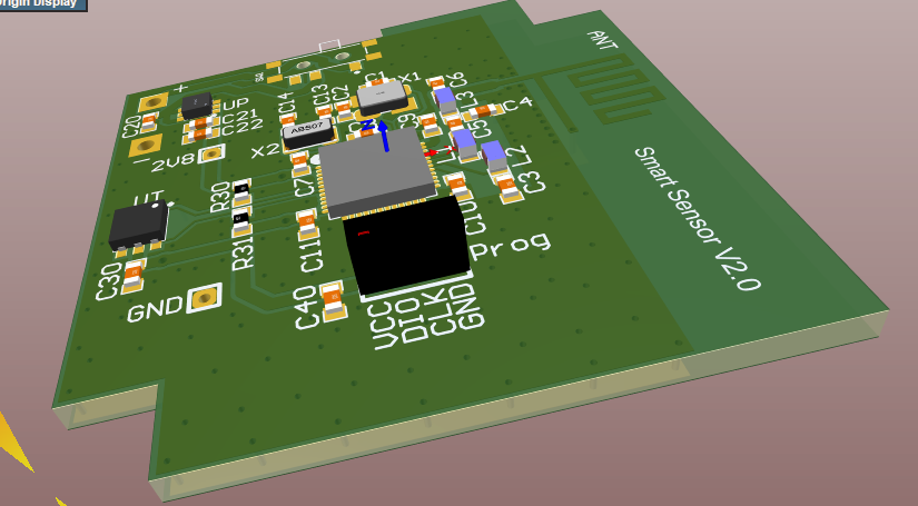

BleTemperaturesensor

BleTemperaturesensor
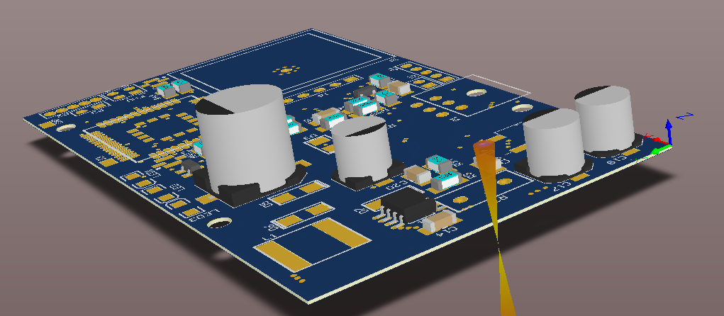

Personal tracking system

Personal tracking system
Pcb Layout of Automatic hand sanitizer.
Pcb Layout of Automatic hand sanitizer.
BleTemperaturesensor
BleTemperaturesensor
Personal tracking system
Personal tracking system
Reviews
Changes saved
Showing 1 - 2 out of 2 reviews
$217.49 USD
PCB Layout
T
•
$27.00 USD
Electronics
Microcontroller
Electrical Engineering
PCB Layout
Circuit Design
T
•
Experience
design single side, double sided and multilayered PCBs
Oct 2006 - Present
1. Worked on design single side, double sided and multilayered PCBs using industry standard techniques.
2. Generate and maintain Gerber and CAM.
3. CAD library administration including symbol, footprint generation and database administration.
4. BOM preparation.
5. Gerber / ODB++ files(Fabrication/Assembly files) Validate by using Valor Genesis 2000 & CAM350
Education
B.E In EC
(4 years)
Contact Maulik P. about your job
Log in to discuss any details over chat.
Verifications
Top Skills
Browse Similar Freelancers
Browse Similar Showcases
Invite sent successfully!
Thanks! We’ve emailed you a link to claim your free credit.
Something went wrong while sending your email. Please try again.
Copy to clipboard failed, please try again after adjusting your permissions.
Copied to clipboard.
Loading preview
Permission granted for Geolocation.
Your login session has expired and you have been logged out. Please log in again.